1.0 Research Title:
To investigate the applicability of using GaN power Integrated-circuits in supporting high-frequency power switching applications
2.0 Abstract
GaN is a binary III-V direct bandgap semiconductor(Levinshtein, Rumyantsev & Shur, 2001). GAN transistor is often used for high power and high-frequency devices because it has a wide band gap of 3.4 eV. Moreover, GaN also provides high bread-down voltages, high electron mobility, and saturation velocity. As such, it is also an ideal alternative for high-power and high-temperature microwave applications like high-voltage switching devices for power grids. GaN stands for Gallium Nitride. It is evolved from Gallium Arsenide or GaAs. According to Xing, et al.(2004), GaN transistors have many advantages including high-operating voltage, high operating temperature, high power density, durable and crack-resistant material. However, meanwhile, it should also be noticed that GaN materials have many potential limitations such as high density of defect rates. At present, many manufacturers still prefer to use SiC transistors. Wolfspeed, Rohm, Infineon, ST Micro, etc, are still producing SiC semiconductor materials to produce diodes and transistors (Liu et al., 2016). It is largely because SiC can support relatively strong electric field at high breakdown voltage. SiC also has good thermal conductivity and thus can work at very high temperature. As compared with SiC, GaN has a much higher electron mobility. In other words, manufacturers can enjoy low cost of production. The research interest of this study is to conduct an in-depth analysis on the applicability of GaN power IC technology in supporting high-frequency power switching applications. Previously, GaN power IC technology particular in terms of the D-HEMT and E-HEMT structure have been proven to be effective in making high-voltage power switching devices(Bindra, 2018). Several E-HEMT transistors have already entered the market. It is also expected that the market size of E-HEMT GaN transistors will be larger and larger. However, meanwhile, there are still many problems associated with the E-HEMT GaN IC technology. The voltage oscillations created by the current PCB design and the interconnections of electric components remarkably reduce the reliability of the GaN transistors. The gate drive margins of commercial GaN is still inferior to SiC.
3.0 Aim
The objective of this research is to investigate the applicability of using GaN power IC technology in supporting high-frequency power switching devices. It is necessary and meaningful to modify the current configuration of the GaN heterojunction structure such as the E-HEMT to reduce the negative effect of voltage oscillation and make it possible for high-density of integration among different devices(Lanford et al., 2005).
4.0 Literature Review
4.1 Power-switch Requirements and Limitations of Silicon Devices
There are mainly two types of switches in switch-mode integrated circuits, namely diodes and transistors. Diodes are two-terminal rectifiers. Transistors, on the other hand, are three-terminal controlled switches. Materials need to fulfil two key power-switch requirements in order to be used in diodes and transistors. First, it needs to have blocking voltage. Second, the switching speed also needs to be very fast. The normal-off switch is off when the applied voltage is zero. The switch is on when there is a positive controlled voltage. The relationship between blocking voltage and electric field can be illustrated in the formula below(Okuto & Crowell, 1975),
Vb = εsE/(2qND).......................................................(1)
Vb denotes blocking voltage. E is the maximum electric field that can be supported by the selected material. Nd stands for the lower doping of the drift region. The thickness of the drift region, LN should not be thinner than the depletion layer, wd as shown in the formula below,
LN ≈ wd = Sqr (2εs Vb/qNd)................................(2)
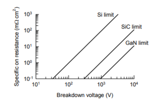
From equation (1) and (2), it is not difficult to observe that a higher blocking voltage Vb requires a thicker drift region. Vb is positively correlated with LN. It will further result in a longer resistor with thick drift region when the switching device is turned on. Moreover, according to Wei (2020), the specific “on” resistance is also positively correlated with the blocking voltage because resistance is directly proportionate to LN. Assume that 10A current is in “on” mode. The active area of the switching device is 1 cm2. Li et al.(2000) found that for a specific resistance of 100 mΩ*cm2, the “on” resistance will be 0.1 Ω. 1 volt decrease will lead to a power loss of 10W. In other words, the electric field supported by a material will limit the blocking voltage in the operations. Silicon devices, for instance, can only have a maximum 1,000 V. There is no way to exceed this limit. According to Deboy et al. (2016), the blocking voltage of three major materials including Si, SiC and GaN can be shown in the figure 1 below. It can be observed that GaN as compared with Si and SiC has a much higher breakdown voltage limit.

Source Credit:Deboy et al., 2016
Fig 1: Breakdown voltage limits of Si, SiC and GaN
The second requirement is high switching speed. High switching speed is equivalent to smaller size of inductors and lower cost. In this sense, Schotty diodes are much bettern than conventional P-N junction diodes largely because the unipolar design potentially avoids the switching delay (Chen et al., 2011). In other words, the switching speed is much faster. However, in reality, a Schott diodes has very low breakdown voltage. Thus, manufacturers have to choose P-N junctions to make diodes and transistors.
4.2 GaN Transistors
Like the aforementioned, semi-conductor materials need to withstand a much higher electric field in order to be used for switching devices. In other words, these materials need to have high breakdown voltage. In the last century, SiC was used for power switches because it had a relatively high breakdown voltage at that time. As compared Si materials, the breakdown electric field of SiC is about 200~300 V/ᵤm. The breakdown voltage of SiC is almost 10 times higher than Si materials. Besides, the thermal conductivity of SiC is about 3 times higher than Si. SiC Schotty diodes (unipolar) could thus work under much higher temperature. CREE is the first company commercialized the SiC Schotty diodes (Wang et al., 2013). As compared with Si P-N junctions, the SiC Schotty diodes have a much higher price. But the fast switching speed is the major highlight. Even at present, there are still some producers like Infineon and Rohm who use SiC to produce diodes and transistors. According to Hazra et al.(2015), if the requirement for breakdown voltage of 1,700 V and above, SiC Shotty Diodes are still the best choice.
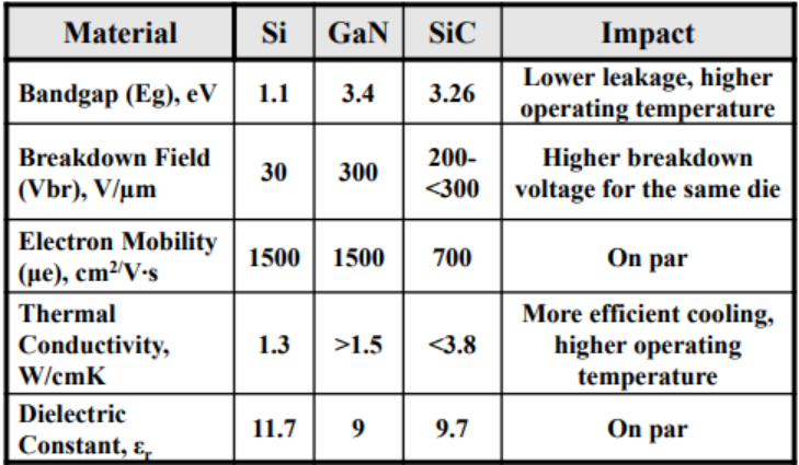
However, as compared to SiC materials, GaN can withstand even higher electric field. GaN has a very large band-gap of 3.4 eV as shown in Table 1 below. A large band-gap means that there will be lower leakage and higher operating temperature. The breakdown field of GaN is about 300 V/ᵤm.
Table 1: Comparison among Si, GaN and SiC semi-conductor materials

Source Credit: Xing, et al., 2004
GaN device often grows on SiC substrates. The GaN-on-Si power devices have a very fast switching speed at low conduction loss(Chen et al., 2017). GaN’s wide band-gap, like the aforementioned, can allow for higher breakdown voltages at very high temperature. Meanwhile, SiC as compared with pure silicon has much better heat capacity and thermal conductivity. The pure form of GaN can effectively resist cracking and deposited on SiC. However, GaN has a critical problem of a high spatial defect frequency. When grown on Silicon Carbide wafers, GaN exhibits very high density of defects as high as 108 cm-2. it is even more expensive than SiC itself. As such, GaN-on-Si is often not used for power-electronic devices. Instead, according to Zhang et al.(2003), the high density of defects does not cause fatal short circuits. Therefore, GaN can be used for limit-emitting operations as the defects are not fatal. Besides, GaN grown on Si substrates have been developed and commercialized for microwave applications. Even though the density of defects is very high, manufacturers still decide to produce GaN grown in Si substrates. It is largely because Si substrate is very much cheaper.
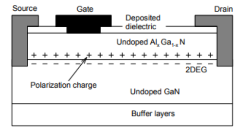
The commercialized power transistors in GaN is based on a structure called HEMT. It stands for High Electron Mobility Transistor. The electron mobility in HEMT is typically 2000 cm2/Vs. The electron mobility is about 100 times higher than SiC substrate. Therefore, it is expected that HEMT will have a potential advantage over other types of substrates in the future high-frequency switching microwave applications. The high electron mobility of GaN is attributed to the electron channel formed between undoped GaN and AlGaN as shown in figure 2. The transition from GaN to AlGaN creates fixed and polarized charges that attract electrons from the 2DEG (two-dimensional electron gas). The trap of polarization charges is 2-dimensional due to the quantum confinement of electrons in the energy potential well. The huge electron mobility in the HEMT structure significantly bring down the cost for commercialization.

Fig 2: Cross-section of HEMT structure
4.3 GaN Power IC Technology
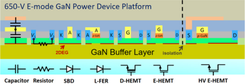
The 2-D nature of GaN HEMT structure provides high-density integration. A commercial GaN-on-Si on p-GaN gate HEMT platform can be shown in the fig 3 below.The high p-GaN gate HEMT can be used as a power switch. In order to be used as a power switch, the GaN HEMT structure should be designed with proper gate-to-drain distance. Hwang et al. (2013) found that for a 650 V p-GaN gate HEMT, the typical on-resistance is about 130mΩ. The gate charge is very low as compared to Si and SiC. In other words, the p-Gan Gate HEMT can have a very fast switching speed.

Source Credit:Wei et al., 2020
Fig 3: GaN power ICs.
5.0 Methodology
In this proposed research, I will comprehensively discuss about the applicability of GaN transistors on the high-frequency power switching. One major challenge is the parasitic inductance for high-frequency switching. The common-source inductance (CSI) acts as a negative feedback which potentially slows down the turn-on and turn-off period. Conventional GaN FET (field-effect transistor) such as HEMT has critical-source inductance its bonding wire. Therefore, the idea of this research is that another bonding wire may be introduced to reduce the CSI. The inductance is created by the source electrode of Si MOSFET and the gate electrode of GaN. The modified design of the bonding wire will be compared and contrasted with the conventional GaN FET. The original GaN FET will be packaged by a To-254 metal package with a conventional cascode structure. The modified structure will be adding an additional bonding wire. The low-voltage source electrode of Si-MOSFET is prepared by Trinno technology. The Threshold voltage is decided to be 5 V. The maximum drain-source current is 50A. Breakdown voltage is set to be 100V. The drain-source resistance is 30mΩ. The size is 2.8 mm X 2.8 mm. The high-voltage depletion-voltage depleting-mode GaN FET will be prepared by ETRI. The gate length is 1 micrometer. The unit gate width is 0.5 mm. The total gate with is 30mm. The gate-to-source distance is 2 micrometer. The threshold voltage of GaN FET is -5.5 V. A maximum drain current is 10A. The drain-breakdown voltage is 600V. The new bonding wire is made of AuSn. Eutectic bonding technique is used to attach the bonding wire onto the To-254 package. Through applying the new GaN power IC technology, the effectiveness of reducing the common-source inductance in the modified GaN FET can be identified. Then, the applicability of the new technology in applying GaN FET in producing high-frequency power switching devices will be future discussed and evaluated.
6.0 Timeline
The first year:Theory learning. I am very interested in learning the functions and characteristics of different semiconductor materials. Even though the research focus is GaN, I want to learn more about other materials as well. Through comparing and contrasting different materials, the advantages and disadvantages of GaN FET can be clearly identified. The potential challenge in GaN FET such as common-source inductance can be learned more deeply in the first year.
The Second year: Learn deeply about GaN power IC technology. Necessary materials should also be prepared in this year. Technologies such as TO-254, Trinno, ETRI, etc, should be effectively mastered by the researcher in the learning process.
The Third year: The dissertation structure should be well presented. During the learning process, the research proposal may be modified further after learning more deeply about the subject. For instance, the GaN FET can be identified as GaN enhancement-mode HEMT. Instead of adding an additional bonding wire, other new modifications may also be introduced into the experiment.
7.0 Reference
Bindra, A. (2018). Wide-bandgap power devices: Adoption gathers momentum. IEEE Power Electronics Magazine, 5(1), 22-27.
Chen, C. C., Aykol, M., Chang, C. C., Levi, A. F. J., & Cronin, S. B. (2011). Graphene-silicon Schottky diodes. Nano letters, 11(5), 1863-1867.
Chen, K. J., Häberlen, O., Lidow, A., lin Tsai, C., Ueda, T., Uemoto, Y., & Wu, Y. (2017). GaN-on-Si power technology: Devices and applications. IEEE Transactions on Electron Devices, 64(3), 779-795.
Deboy, G., Treu, M., Häberlen, O., & Neumayr, D. (2016, December). Si, SiC and GaN power devices: An unbiased view on key performance indicators. In 2016 IEEE International Electron Devices Meeting (IEDM) (pp. 20-2). IEEE.
Hazra, S., De, A., Cheng, L., Palmour, J., Schupbach, M., Hull, B. A.,& Bhattacharya, S. (2015). High switching performance of 1700-V, 50-A SiC power MOSFET over Si IGBT/BiMOSFET for advanced power conversion applications. IEEE transactions on Power Electronics, 31(7), 4742-4754.
Hwang, I., Kim, J., Choi, H. S., Choi, H., Lee, J., Kim, K. Y.,& Shin, J. (2013). p-GaN gate HEMTs with tungsten gate metal for high threshold voltage and low gate current. IEEE electron device letters, 34(2), 202-204.
Levinshtein, M. E., Rumyantsev, S. L., & Shur, M. S. (Eds.). (2001). Properties of Advanced Semiconductor Materials: GaN, AIN, InN, BN, SiC, SiGe. John Wiley & Sons.
Lanford, W. B., Tanaka, T., Otoki, Y., & Adesida, I. (2005). Recessed-gate enhancement-mode GaN HEMT with high threshold voltage. Electronics Letters, 41(7), 449-450.
Liu, T., Ning, R., Wong, T. T., & Shen, Z. J. (2016). Modeling and analysis of SiC MOSFET switching oscillations. IEEE Journal of Emerging and Selected Topics in Power Electronics, 4(3), 747-756.
Li, Y. L., Schubert, E. F., Graff, J. W., Osinsky, A., & Schaff, W. F. (2000). Low-resistance ohmic contacts to p-type GaN. Applied Physics Letters, 76(19), 2728-2730.
Okuto, Y., & Crowell, C. R. (1975). Threshold energy effect on avalanche breakdown voltage in semiconductor junctions. Solid-State Electronics, 18(2), 161-168.
Wei, J., Tang, G., Xie, R., & Chen, K. J. (2020). GaN power IC technology on p-GaN gate HEMT platform. Japanese Journal of Applied Physics, 59(SG), SG0801.
Wang, G., Wang, F., Magai, G., Lei, Y., Huang, A., & Das, M. (2013, September). Performance comparison of 1200V 100A SiC MOSFET and 1200V 100A silicon IGBT. In 2013 IEEE Energy Conversion Congress and Exposition (pp. 3230-3234). IEEE.
Xing, H., Dora, Y., Chini, A., Heikman, S., Keller, S., & Mishra, U. K. (2004). High breakdown voltage AlGaN-GaN HEMTs achieved by multiple field plates. IEEE Electron Device Letters, 25(4), 161-163.
Zhang, A. P., Rowland, L. B., Kaminsky, E. B., Tilak, V., Grande, J. C., Teetsov, J.,& Eastman, L. F. (2003). Correlation of device performance and defects in AlGaN/GaN high-electron mobility transistors. Journal of electronic materials, 32(5), 388-394.